EVAL-AD5541ASDZ View Datasheet(PDF) - Analog Devices
Part Name
Description
MFG CO.
'EVAL-AD5541ASDZ' PDF : 20 Pages View PDF
Data Sheet
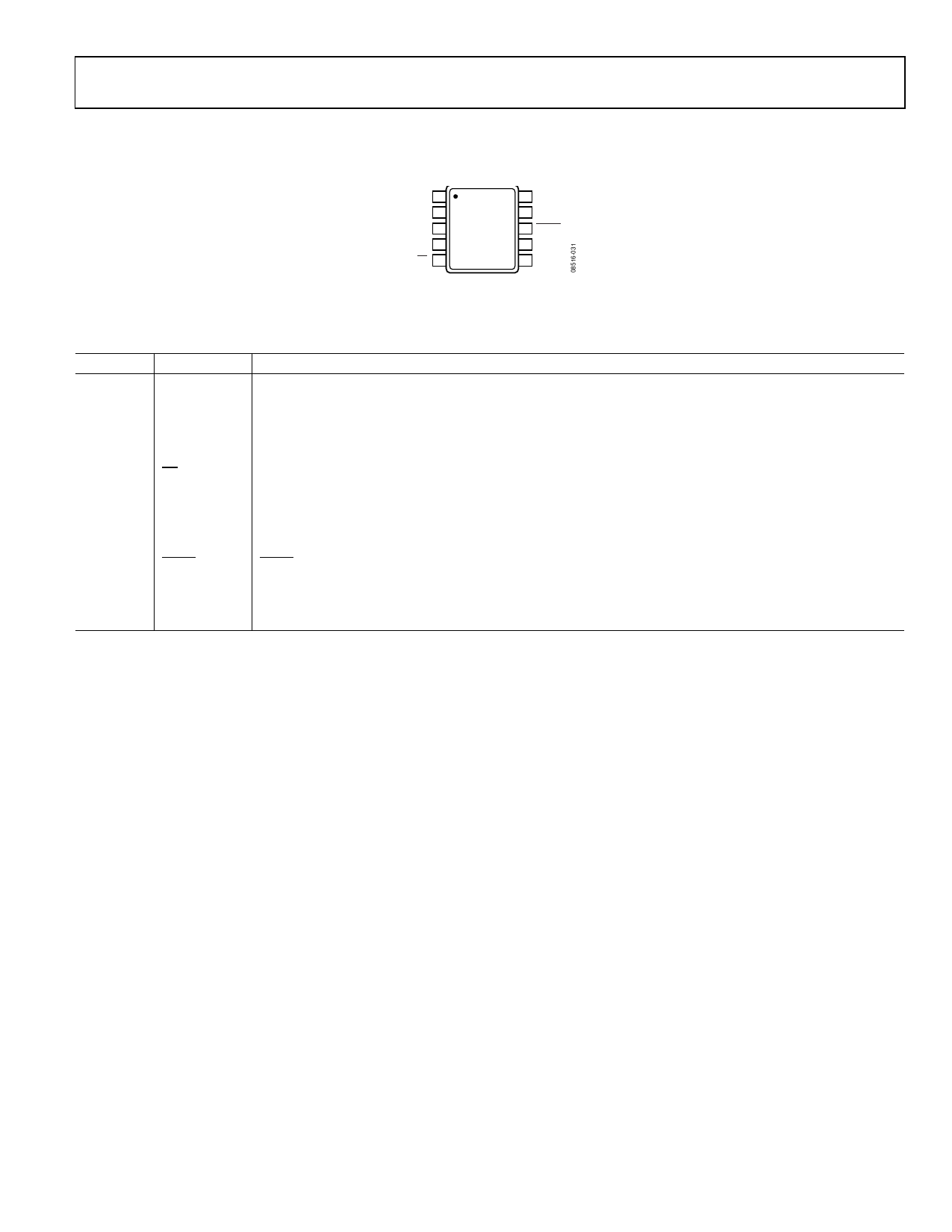
PIN CONFIGURATIONS AND FUNCTION DESCRIPTIONS
AD5541A
VDD 1
VOUT 2
AGND 3
REF 4
CS 5
AD5541A
TOP VIEW
(Not to Scale)
10 VLOGIC
9 DGND
8 LDAC
7 DIN
6 SCLK
Figure 4. AD5541A 10-Lead MSOP Pin Configuration
Table 6. AD5541A Pin Function Descriptions
Pin No. Mnemonic Description
1
VDD
Analog Supply Voltage.
2
VOUT
Analog Output Voltage from the DAC.
3
AGND
Ground Reference Point for Analog Circuitry.
4
REF
Voltage Reference Input for the DAC. Connect to an external 2.5 V reference. The reference can range from
2 V to VDD.
5
CS
Logic Input Signal. The chip select signal is used to frame the serial data input.
6
SCLK
Clock Input. Data is clocked into the serial input register on the rising edge of SCLK. The duty cycle must be
between 40% and 60%.
7
DIN
Serial Data Input. This device accepts 16-bit words. Data is clocked into the serial input register on the rising edge
of SCLK.
8
LDAC
LDAC Input. When this input is taken low, the DAC register is simultaneously updated with the contents of the
serial register data.
9
DGND
Digital Ground. Ground reference for digital circuitry.
10
VLOGIC
Logic Power Supply.
Rev. B | Page 7 of 20
Share Link: 
